- 您现在的位置:买卖IC网 > Sheet目录3878 > PIC18F4610T-I/ML (Microchip Technology)IC MCU FLASH 32KX16 44QFN
2009 Microchip Technology Inc.
DS39636D-page 33
PIC18F2X1X/4X1X
2.8
Effects of Power-Managed Modes
on the Various Clock Sources
When PRI_IDLE mode is selected, the designated
primary oscillator continues to run without interruption.
For all other power-managed modes, the oscillator
using the OSC1 pin is disabled. The OSC1 pin (and
OSC2 pin, if used by the oscillator) will stop oscillating.
In
Secondary
Clock
modes
(SEC_RUN
and
SEC_IDLE), the Timer1 oscillator is operating and
providing the device clock. The Timer1 oscillator may
also run in all power-managed modes if required to
clock Timer1 or Timer3.
In Internal Oscillator modes (RC_RUN and RC_IDLE),
the internal oscillator block provides the device clock
source. The 31 kHz INTRC output can be used directly
to provide the clock and may be enabled to support
various special features, regardless of the power-
managed mode (see Section 22.2 “Watchdog Timer
information on WDT, Fail-Safe Clock Monitor and Two-
Speed Start-up). The INTOSC output at 8 MHz may be
used directly to clock the device or may be divided
down by the postscaler. The INTOSC output is disabled
if the clock is provided directly from the INTRC output.
If the Sleep mode is selected, all clock sources are
stopped. Since all the transistor switching currents
have been stopped, Sleep mode achieves the lowest
current consumption of the device (only leakage
currents).
Enabling any on-chip feature that will operate during
Sleep will increase the current consumed during Sleep.
The INTRC is required to support WDT operation. The
Timer1 oscillator may be operating to support a real-
time clock. Other features may be operating that do not
require a device clock source (i.e., SSP slave, PSP,
INTn pins and others). Peripherals that may add
significant
current
consumption
are
listed
in
Section 25.2 “DC Characteristics”.
2.9
Power-up Delays
Power-up delays are controlled by two timers, so that
no external Reset circuitry is required for most applica-
tions. The delays ensure that the device is kept in
Reset until the device power supply is stable under nor-
mal circumstances and the primary clock is operating
and stable. For additional information on power-up
delays, see Section 4.5 “Device Reset Timers”.
The first timer is the Power-up Timer (PWRT), which
provides a fixed delay on power-up (parameter 33,
Table 25-10). It is enabled by clearing (= 0) the
PWRTEN Configuration bit.
The second timer is the Oscillator Start-up Timer
(OST), intended to keep the chip in Reset until the
crystal oscillator is stable (LP, XT and HS modes). The
OST does this by counting 1024 oscillator cycles
before allowing the oscillator to clock the device.
When the HSPLL Oscillator mode is selected, the
device is kept in Reset for an additional 2 ms, following
the HS mode OST delay, so the PLL can lock to the
incoming clock frequency.
Table 25-10), following POR, while the controller
becomes ready to execute instructions. This delay runs
concurrently with any other delays. This may be the
only delay that occurs when any of the EC, RC or INTIO
modes are used as the primary clock source.
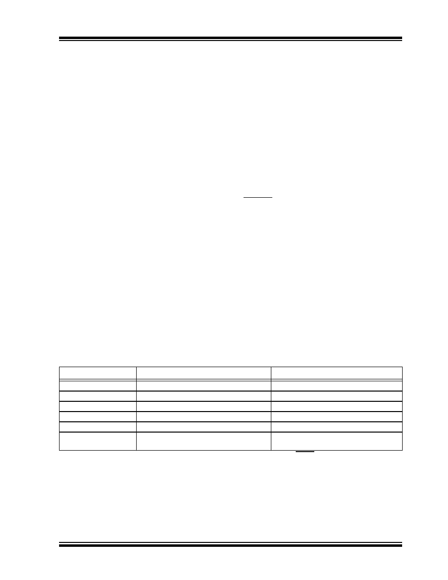
TABLE 2-3:
OSC1 AND OSC2 PIN STATES IN SLEEP MODE
Oscillator Mode
OSC1 Pin
OSC2 Pin
RC, INTIO1
Floating, external resistor should pull high
At logic low (clock/4 output)
RCIO
Floating, external resistor should pull high
Configured as PORTA, bit 6
INTIO2
Configured as PORTA, bit 7
Configured as PORTA, bit 6
ECIO
Floating, pulled by external clock
Configured as PORTA, bit 6
EC
Floating, pulled by external clock
At logic low (clock/4 output)
LP, XT and HS
Feedback inverter disabled at quiescent
voltage level
Feedback inverter disabled at quiescent
voltage level
Note:
See Table 4-2 in Section 4.0 “Reset” for time-outs due to Sleep and MCLR Reset.
发布紧急采购,3分钟左右您将得到回复。
相关PDF资料
PIC18F4610-E/PT
IC MCU FLASH 32KX16 44TQFP
PIC18F4610-E/ML
IC MCU FLASH 32KX16 44QFN
PIC18LF2331T-I/SO
IC MCU FLASH 4KX16 28SOIC
PIC18F4515T-I/PT
IC MCU FLASH 24KX16 44TQFP
PIC18F4431T-I/ML
IC MCU FLASH 8KX16 44QFN
PIC18F4431-E/ML
IC MCU FLASH 8KX16 44QFN
PIC18F4410T-I/ML
IC MCU FLASH 8KX16 44QFN
PIC18F4410-E/PT
IC MCU FLASH 8KX16 44TQFP
相关代理商/技术参数
PIC18F4610T-I/PT
功能描述:8位微控制器 -MCU 64KB 3968 RAM 36 I/O RoHS:否 制造商:Silicon Labs 核心:8051 处理器系列:C8051F39x 数据总线宽度:8 bit 最大时钟频率:50 MHz 程序存储器大小:16 KB 数据 RAM 大小:1 KB 片上 ADC:Yes 工作电源电压:1.8 V to 3.6 V 工作温度范围:- 40 C to + 105 C 封装 / 箱体:QFN-20 安装风格:SMD/SMT
PIC18F4620-E/ML
功能描述:8位微控制器 -MCU 64KB 3968 RAM 36 I/O RoHS:否 制造商:Silicon Labs 核心:8051 处理器系列:C8051F39x 数据总线宽度:8 bit 最大时钟频率:50 MHz 程序存储器大小:16 KB 数据 RAM 大小:1 KB 片上 ADC:Yes 工作电源电压:1.8 V to 3.6 V 工作温度范围:- 40 C to + 105 C 封装 / 箱体:QFN-20 安装风格:SMD/SMT
PIC18F4620-E/P
功能描述:8位微控制器 -MCU 64KB 3968 RAM 36 I/O RoHS:否 制造商:Silicon Labs 核心:8051 处理器系列:C8051F39x 数据总线宽度:8 bit 最大时钟频率:50 MHz 程序存储器大小:16 KB 数据 RAM 大小:1 KB 片上 ADC:Yes 工作电源电压:1.8 V to 3.6 V 工作温度范围:- 40 C to + 105 C 封装 / 箱体:QFN-20 安装风格:SMD/SMT
PIC18F4620-E/PT
功能描述:8位微控制器 -MCU 64KB 3968 RAM 36 I/O RoHS:否 制造商:Silicon Labs 核心:8051 处理器系列:C8051F39x 数据总线宽度:8 bit 最大时钟频率:50 MHz 程序存储器大小:16 KB 数据 RAM 大小:1 KB 片上 ADC:Yes 工作电源电压:1.8 V to 3.6 V 工作温度范围:- 40 C to + 105 C 封装 / 箱体:QFN-20 安装风格:SMD/SMT
PIC18F4620-E/PT
制造商:Microchip Technology Inc 功能描述:IC 8BIT MCU PIC18F 40MHZ TQFP-44 制造商:Microchip Technology Inc 功能描述:IC, 8BIT MCU, PIC18F, 40MHZ, TQFP-44
PIC18F4620-I/ML
功能描述:8位微控制器 -MCU 64KB 3968 RAM 36 I/O RoHS:否 制造商:Silicon Labs 核心:8051 处理器系列:C8051F39x 数据总线宽度:8 bit 最大时钟频率:50 MHz 程序存储器大小:16 KB 数据 RAM 大小:1 KB 片上 ADC:Yes 工作电源电压:1.8 V to 3.6 V 工作温度范围:- 40 C to + 105 C 封装 / 箱体:QFN-20 安装风格:SMD/SMT
PIC18F4620-I/P
功能描述:8位微控制器 -MCU 64KB 3968 RAM 36 I/O RoHS:否 制造商:Silicon Labs 核心:8051 处理器系列:C8051F39x 数据总线宽度:8 bit 最大时钟频率:50 MHz 程序存储器大小:16 KB 数据 RAM 大小:1 KB 片上 ADC:Yes 工作电源电压:1.8 V to 3.6 V 工作温度范围:- 40 C to + 105 C 封装 / 箱体:QFN-20 安装风格:SMD/SMT
PIC18F4620-I/P
制造商:Microchip Technology Inc 功能描述:IC 8BIT FLASH MCU 18F4620 DIP40